- 您现在的位置:买卖IC网 > Sheet目录3878 > PIC18F258T-I/SOG (Microchip Technology)IC MCU FLASH 16KX16 28SOIC
2006 Microchip Technology Inc.
DS41159E-page 15
PIC18FXX8
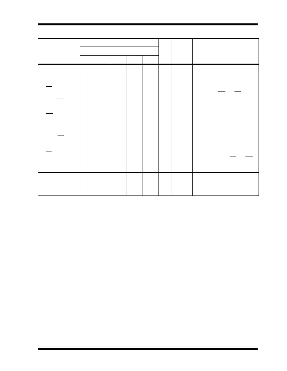
PORTE is a bidirectional I/O port.
RE0/AN5/RD
RE0
AN5
RD
—8
25
9
I/O
I
ST
Analog
TTL
Digital I/O.
Analog input 5.
Read control for Parallel Slave
Port (see WR and CS pins).
RE1/AN6/WR/C1OUT
RE1
AN6
WR
C1OUT
—9
26
10
I/O
I
O
ST
Analog
TTL
Analog
Digital I/O.
Analog input 6.
Write control for Parallel Slave
Port (see CS and RD pins).
Comparator 1 output.
RE2/AN7/CS/C2OUT
RE2
AN7
CS
C2OUT
—10
27
11
I/O
I
O
ST
Analog
TTL
Analog
Digital I/O.
Analog input 7.
Chip select control for Parallel
Slave Port (see RD and WR
pins).
Comparator 2 output.
VSS
19, 8
12, 31
6, 29
13, 34
—
Ground reference for logic and
I/O pins.
VDD
20
11, 32
7, 28
12, 35
—
Positive supply for logic and I/O
pins.
TABLE 1-2:
PIC18FXX8 PINOUT I/O DESCRIPTIONS (CONTINUED)
Pin Name
Pin Number
Pin
Type
Buffer
Type
Description
PIC18F248/258
PIC18F448/458
SPDIP, SOIC
PDIP
TQFP
PLCC
Legend: TTL = TTL compatible input
CMOS = CMOS compatible input or output
ST
= Schmitt Trigger input with CMOS levels
Analog = Analog input
I
= Input
O
= Output
P
= Power
OD
= Open-Drain (no P diode to VDD)
发布紧急采购,3分钟左右您将得到回复。
相关PDF资料
PIC18F2515T-I/SO
IC MCU FLASH 24KX16 28SOIC
PIC16LF1933-I/SP
IC PIC MCU FLASH 4K 28-DIP
PIC18F2515-E/SP
IC MCU FLASH 24KX16 28-DIP
PIC18F23K20-I/SP
IC PIC MCU FLASH 4KX16 28-DIP
PIC18F2515-E/SO
IC MCU FLASH 24KX16 28SOIC
PIC24F08KL401-I/MQ
IC MCU 16BIT 8KB FLASH 20-QFN
PIC16C55A-04/SP
IC MCU OTP 512X12 28DIP
PIC18F2431T-I/ML
IC MCU FLASH 8KX16 28QFN
相关代理商/技术参数
PIC18F25J10-I/ML
功能描述:8位微控制器 -MCU 32 KB FL 1024 RAM RoHS:否 制造商:Silicon Labs 核心:8051 处理器系列:C8051F39x 数据总线宽度:8 bit 最大时钟频率:50 MHz 程序存储器大小:16 KB 数据 RAM 大小:1 KB 片上 ADC:Yes 工作电源电压:1.8 V to 3.6 V 工作温度范围:- 40 C to + 105 C 封装 / 箱体:QFN-20 安装风格:SMD/SMT
PIC18F25J10-I/SO
功能描述:8位微控制器 -MCU 32 KB FL 1024 RAM RoHS:否 制造商:Silicon Labs 核心:8051 处理器系列:C8051F39x 数据总线宽度:8 bit 最大时钟频率:50 MHz 程序存储器大小:16 KB 数据 RAM 大小:1 KB 片上 ADC:Yes 工作电源电压:1.8 V to 3.6 V 工作温度范围:- 40 C to + 105 C 封装 / 箱体:QFN-20 安装风格:SMD/SMT
PIC18F25J10-I/SP
功能描述:8位微控制器 -MCU 32 KB FL 1024 RAM RoHS:否 制造商:Silicon Labs 核心:8051 处理器系列:C8051F39x 数据总线宽度:8 bit 最大时钟频率:50 MHz 程序存储器大小:16 KB 数据 RAM 大小:1 KB 片上 ADC:Yes 工作电源电压:1.8 V to 3.6 V 工作温度范围:- 40 C to + 105 C 封装 / 箱体:QFN-20 安装风格:SMD/SMT
PIC18F25J10-I/SS
功能描述:8位微控制器 -MCU 16 KB FL 1 KB RAM RoHS:否 制造商:Silicon Labs 核心:8051 处理器系列:C8051F39x 数据总线宽度:8 bit 最大时钟频率:50 MHz 程序存储器大小:16 KB 数据 RAM 大小:1 KB 片上 ADC:Yes 工作电源电压:1.8 V to 3.6 V 工作温度范围:- 40 C to + 105 C 封装 / 箱体:QFN-20 安装风格:SMD/SMT
PIC18F25J10T-I/ML
功能描述:8位微控制器 -MCU 32 KB FL 1024 RAM RoHS:否 制造商:Silicon Labs 核心:8051 处理器系列:C8051F39x 数据总线宽度:8 bit 最大时钟频率:50 MHz 程序存储器大小:16 KB 数据 RAM 大小:1 KB 片上 ADC:Yes 工作电源电压:1.8 V to 3.6 V 工作温度范围:- 40 C to + 105 C 封装 / 箱体:QFN-20 安装风格:SMD/SMT
PIC18F25J10T-I/SO
功能描述:8位微控制器 -MCU 32 KB FL 1024 RAM RoHS:否 制造商:Silicon Labs 核心:8051 处理器系列:C8051F39x 数据总线宽度:8 bit 最大时钟频率:50 MHz 程序存储器大小:16 KB 数据 RAM 大小:1 KB 片上 ADC:Yes 工作电源电压:1.8 V to 3.6 V 工作温度范围:- 40 C to + 105 C 封装 / 箱体:QFN-20 安装风格:SMD/SMT
PIC18F25J10T-I/SS
功能描述:8位微控制器 -MCU 16 KB FL 1 KB RAM RoHS:否 制造商:Silicon Labs 核心:8051 处理器系列:C8051F39x 数据总线宽度:8 bit 最大时钟频率:50 MHz 程序存储器大小:16 KB 数据 RAM 大小:1 KB 片上 ADC:Yes 工作电源电压:1.8 V to 3.6 V 工作温度范围:- 40 C to + 105 C 封装 / 箱体:QFN-20 安装风格:SMD/SMT
PIC18F25J11-I/ML
功能描述:8位微控制器 -MCU 32KB Flash 4KBRAM 12MIPS nanoWatt RoHS:否 制造商:Silicon Labs 核心:8051 处理器系列:C8051F39x 数据总线宽度:8 bit 最大时钟频率:50 MHz 程序存储器大小:16 KB 数据 RAM 大小:1 KB 片上 ADC:Yes 工作电源电压:1.8 V to 3.6 V 工作温度范围:- 40 C to + 105 C 封装 / 箱体:QFN-20 安装风格:SMD/SMT